TSMC Runs Five 2nm Fabs as Yield Gap Determines Foundry Leadership
TSMC's five 2nm fabs are selling every wafer through 2026 while Samsung and Intel struggle with yields, making defect density the defining factor in the advanced chip race.
 taipeitimes.com
In this article
66.2%. That is the gross margin TSMC reported for the first quarter of 2026 on April 16, a figure that landed 120 basis points above the upper end of company guidance. It is the highest margin among all pure-play foundries by more than 20 points, and it exists because N2 wafers are sold out through December. Not mostly sold. Not allocated. Sold. Every wafer that will emerge from five Kaohsiung fabs before the calendar flips has a purchase order attached to it.
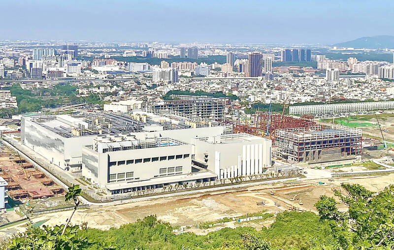
The scale of the N2 ramp is hard to overstate. TSMC is now running five fabrication plants in Kaohsiung dedicated to its 2nm process node, the largest simultaneous single-node buildout in the company's history. According to a Morning Overview report on MSN published May 6, the company will spend between $52 billion and $56 billion in capital expenditure this year, nearly all of it directed at advanced node capacity. Apple alone has secured more than half of TSMC's 2nm output for 2026, locking in multi-year HBM memory supply agreements alongside the logic allocation. Google, Qualcomm, and the hyperscalers are carving up what remains.
And yet the number that actually matters, the one nobody outside Hsinchu will confirm on the record, is the N2 defect density. Process integration engineers I've spoken with place early HVM D0 somewhere in the low 0.3s per square centimeter, which is better than N3 was at the same point in its ramp but worse than the 0.1-something TSMC's automotive-qualification customers want to see. The gap between these two numbers, roughly 0.15 to 0.20 defects per square centimeter, is what determines who ships in volume in Q3 2026 and who waits.
What N2 chose not to be good at, and what TSMC has been unusually candid about, is SRAM scaling. At the N2 technology symposium session in Santa Clara last month, the company confirmed that the high-density SRAM bit-cell on N2 shrinks by roughly 5% versus N3E, well below the historical node-over-node reduction of 15-20%. L3 caches on N2 SoCs will be physically large and will require more area than design teams initially budgeted. The architecture absorbs this; the mask cost does not. A full N2 mask set now runs north of $80 million, and a shuttle run, the kind mid-size chip developers use to qualify IP, costs over $3 million per insertion.
Samsung SF2: GAA is working, yields are not
Across the East China Sea, Samsung Electronics is nearing a technical milestone it has chased since 2022: gate-all-around nanosheet transistors in volume production. Its SF2 process, the commercial name for the 2nm GAA node, has functional silicon. The Exynos 2600, Samsung's first internally designed chip on SF2, has appeared in Geekbench 6 databases running at clocks that suggest the transistor performance is real. But yields, according to a DigiTimes report by Sherri Wang published April 14, remain below the threshold required for stable mass production. Multiple sources cited in that report place the defect density high enough that a significant fraction of candidate smartphone SoC die exiting Samsung's Hwaseong S3 line are non-functional at target clocks.
The GAA nanosheet architecture itself is not the problem. The problem is process control across the nanosheet width, which on SF2 measures between 12nm and 35nm depending on the cell. At those dimensions, a 2nm variation in sheet thickness, the kind of within-wafer non-uniformity that finFET tolerates without visible parametric shift, produces a measurable Vt delta. Samsung's process integration team has spent the past twelve months chasing this with multi-patterning adjustments and deeper source-drain epitaxy optimisation. The downstream effect is visible in the Exynos 2600 power numbers: Gizmochina reported in March that the chip draws approximately 40% more power than the Snapdragon 8 Elite Gen 5 at peak load in Geekbench 6 decompression workloads. That is not a process node performing to specification. That is a process node leaking.
Samsung is not standing still. The company has begun installing advanced equipment at its $17 billion Taylor, Texas plant, a move that signals it expects SF2 yields to become commercially viable and wants U.S.-based capacity ready when they do. And Qualcomm, according to a Fudzilla report from April 21, has been evaluating SF2 for a future Snapdragon flagship, a reversal from the post-Snapdragon 8 Gen 1 era when the company shifted almost exclusively to TSMC. The logic is straightforward: if TSMC cannot supply enough N2 wafers, a second source, even with worse parametric yields, becomes better than no source at all.
Intel 18A: the politics of foundry trust
Intel's foundry business booked $5.4 billion in revenue in Q1 2026, up 16% year on year, a number the company's investor relations team was eager to highlight during the April 23 earnings call. The company described the quarter as showing 'tangible progress' in its foundry segment, with CFO David Zinsner noting that external customer revenue had doubled from the prior year, albeit from a small base. Most of that revenue is still packaging, not leading-edge logic. But the story changed on May 5, when 9to5Mac's Marcus Mendes reported that Apple is in early-stage talks with Intel about using its U.S.-based foundry services for core processor production. Intel shares jumped 15% on the news.
The Apple-Intel conversations are political as much as they are technical. Apple's A-series and M-series chips are designed in Cupertino, manufactured in Taiwan, and imported into the United States under a tariff regime that has become unpredictable. Producing those chips in an Intel fab in Arizona solves a supply-chain geography problem that no amount of process node leadership can address. But Intel 18A, the node on which Apple would hypothetically run its silicon, is still finding its footing. Mass production of Panther Lake on 18A began in late 2025 at Intel's Arizona fab, and the company claims defect density is improving on schedule. What 'on schedule' means in practice, according to process engineers I've spoken with who track Intel's foundry roadmap, is D0 roughly equivalent to where TSMC's N3 was six months before the first iPhone 15 Pro shipped, usable but not comfortable.
What 18A chose not to be good at is power-performance-area competitiveness at the high-performance mobile envelope. Intel's process is optimised for server and client CPU workloads where thermal budgets are north of 45W and clock targets are lower than smartphone SoC peaks. Porting an A-series design, which is tuned for a 5-8W envelope with aggressive burst clocks, onto 18A would require significant re-characterisation of the standard cell libraries and likely a re-spin of the power delivery network. That is not a trivial engineering exercise; it is eighteen months of work before the first test chip tapes out.
The Semiconductor Engineering special report published April 30 by Ann Mutschler frames the broader dynamic clearly: foundry capacity is now the binding constraint on who gets to compete at leading-edge nodes. The report quotes sources across the EDA and fabless ecosystem who describe a world in which N2 and N3 wafer starts are simply unavailable to companies below a certain revenue threshold. A mid-size chip developer with a $200 million annual silicon budget cannot get an N2 shuttle slot before Q2 2027. The capacity has been pre-sold to Apple, Nvidia, AMD, and the hyperscalers. Everyone else is designing for N3E or, increasingly, for Samsung.
The inability to utilize leading-edge process nodes has created opportunities for small and midsize chip developers in multi-die design, along with some sophisticated architectural design tradeoffs., Ann Mutschler, senior executive editor, Semiconductor Engineering
This constraint is reshaping architectural decisions in real time. ChipAgents, a startup building AI training ASICs, told Semiconductor Engineering that it is designing for a chiplet architecture specifically because it cannot guarantee a leading-edge node allocation for a monolithic reticle-sized die. Baya Systems, a network-on-chip IP vendor, described customers choosing to implement compute dies on N3E and I/O dies on N6, a split that would have been considered inefficient eighteen months ago but is now standard practice. The bottleneck has migrated from design complexity to wafer access, and the response is disaggregation, not because it is elegant but because it is possible.
The supply-side picture at Samsung offers a partial release valve. The Korea Herald reported on March 30 that Samsung is emerging as a 'potential beneficiary' of the tightening supply crunch at TSMC, particularly as AI chip demand continues to outstrip N2 and N3 capacity. Samsung's foundry team has been quietly qualifying its SF2 process with a handful of mid-tier customers who cannot get TSMC allocation. One of those customers, according to industry sources, is an autonomous driving chip startup that needs a sub-5nm process for its next-generation inference accelerator and has been told by TSMC that the earliest N3E shuttle is Q4 2026. Samsung can offer a Q3 2026 SF2 shuttle. The yield risk is higher, but for a startup whose entire roadmap depends on shipping silicon by mid-2027, the choice is not between good yield and bad yield; it is between some yield and no silicon at all.
Intel's foundry qualification challenge is different. The company has the process, the fabs, and now, with the Apple talks, the potential anchor customer. What it lacks is the EDA ecosystem maturity and the IP library depth that TSMC has spent two decades building. A design team moving from TSMC N5 to Intel 18A must re-qualify every memory compiler, every SerDes macro, every standard cell. That takes multiple test-chip iterations and a foundry customer-support apparatus that Intel is still building. The company's foundry services group has hired aggressively from TSMC and Samsung over the past eighteen months, but culture and process maturity are not hired; they are accumulated.
The equipment supply chain is tightening across all three foundries, and the pinch point is ASML's high-NA EUV tools. TSMC has taken delivery of its first two Twinscan EXE:5200 systems for N2 development and is expected to deploy high-NA at scale for the A14 node in 2028. Intel has been more aggressive, installing high-NA systems at its Oregon development fab and using them for 18A patterning on selective layers. Samsung's high-NA strategy is less visible; the company has ordered the tools but has not disclosed a deployment timeline. The equipment constraint means that even if Samsung solved its SF2 yield problem tomorrow, it could not match TSMC's N2 wafer output before 2028 at the earliest. The capacity gap is capital-locked, not just know-how-locked.
For the fabless chip industry, the message of the first half of 2026 is unambiguous: the leading edge has become a members-only club, and the membership fee is a multi-billion-dollar wafer commitment. TSMC's five-fab N2 buildout, far from creating surplus capacity, has merely kept pace with the demand from its three largest customers. Samsung's SF2 yields, while improving, have not yet crossed the line where a risk-averse procurement team at a major smartphone OEM would commit a flagship socket. And Intel's 18A is technically viable, politically attractive, and still eighteen to twenty-four months away from being a genuine third option for anyone whose purchasing department is not also reading geopolitical intelligence briefings.
The next checkpoint is TSMC's Q2 2026 earnings call, scheduled for July 16. By then, we will know whether N2 defect density has moved from the low 0.3s into the 0.2s, the range where Apple's iPhone 19 Pro volume ramp becomes a question of capacity, not yield. Samsung's SF2 customer qualification timeline points to a decision point in late Q3. If yields cross 65-70% by September, expect at least one marquee Android socket to commit. If they do not, SF2 will follow the same trajectory as Samsung's 3nm GAE: a technically impressive demonstration that arrived too late for the volume window. Intel's milestone is softer but more consequential: whether the Apple talks move from exploratory to a memorandum of understanding with a tape-out commitment attached. That announcement, if it comes, will not be during an earnings call. It will arrive on a Friday afternoon, buried in a supply-chain diversification press release, and it will change the foundry order more than any yield chart ever could.
Read next
