Advanced Packaging Becomes Chip Industry's Most Expensive Bottleneck
With CoWoS capacity booked through 2027 and hybrid bonding still emerging, chip designers are scrambling to rework roadmaps around the advanced packaging constraint that nobody saw coming.
 tomshardware.com
Nvidia has reserved the majority of TSMC's most advanced packaging capacity, booking CoWoS lines so far into the future that second-tier AI chip developers cannot get a slot before 2028. The figure, confirmed by CNBC in an April 2026 report, is the clearest signal yet that advanced packaging has moved from a back-end afterthought to the binding constraint on the entire AI chip pipeline. Without it, a finished wafer is just an expensive silicon coaster.
The shift is structural, not cyclical. When TSMC reports that it is running five 2nm fabs simultaneously and that every wafer through 2026 is already sold, the bottleneck is not lithography. It is what happens after the etch tools power down. Chiplets sliced from different process nodes, sourced from different fabs, sometimes from different continents, must be stitched together with interconnect densities that make motherboard traces look like carrier pigeons. The industry's answer to that problem has a name: CoWoS, or Chip-on-Wafer-on-Substrate, TSMC's advanced packaging platform that uses a silicon interposer to connect multiple compute dies and high-bandwidth memory stacks.
CoWoS is not new. TSMC introduced it in 2012. What is new is the scale of demand and the impossibility of substituting around it. CNBC reported that TSMC is accelerating plans to bring advanced packaging to the United States, with a target date of 2029 for a facility in Arizona. Reuters confirmed the timeline, citing company executives. But 2029 is three years away. In AI hardware, three years is a geological age. The gap between now and then is where the fight for packaging alternatives is playing out.
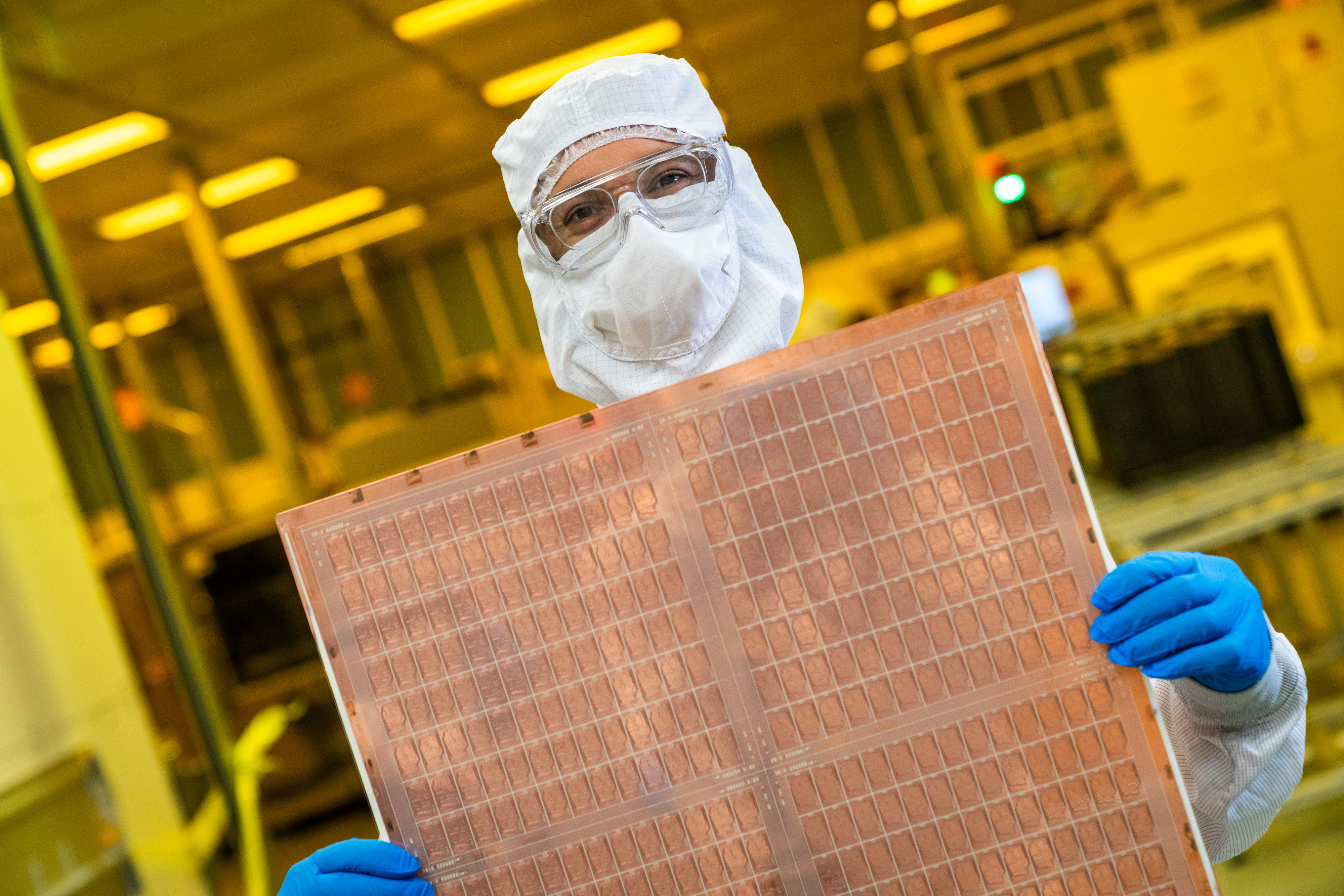
Advanced packaging allows multiple small chips to be connected, protected and tested to create a final larger chip like a graphics processing unit., CNBC, April 2026
Intel sees that gap as an opening. The company's EMIB technology, Embedded Multi-die Interconnect Bridge, embeds a small silicon bridge directly into the organic substrate rather than using a full silicon interposer the size of a reticle. It is a cheaper approach, and Intel is positioning it as the alternative for chip developers locked out of CoWoS. Ars Technica reported in April that Intel's Rio Rancho packaging site in New Mexico, Fab 9 and Fab 11X, has become critical infrastructure for the company's foundry ambitions. The facility was funded in part with $500 million from the US CHIPS Act. Intel CFO Dave Zinsner has signalled that the company is in advanced talks with Google and Amazon for packaging services on custom AI chips, deals that could be worth billions annually, according to 24/7 Wall St.
But EMIB is not a drop-in replacement for CoWoS. The technology trades off interconnect density for cost and substrate compatibility. For the largest AI accelerators, the ones pushing past 6000mm² of total silicon area, a full silicon interposer remains the only viable option. Broadcom made that explicit in December 2024 when it unveiled its 3.5D XDSiP platform, a design that uses TSMC's CoWoS to integrate up to 12 HBM stacks alongside compute logic on a single interposer spanning multiple reticle fields. Tom's Hardware described the platform as enabling 6000mm² of 3D-stacked silicon. The design is not speculative: Broadcom is shipping these packages to hyperscaler customers now.
The dimension that matters here is not just area but bond pitch. CoWoS uses microbumps at pitches around 40 to 50 microns. That has been sufficient for HBM integration and die-to-die links running at a few gigabits per second per pin. But as chiplet counts rise, the interconnect energy per bit becomes the limiting factor. Moving a bit across a 50-micron bump costs roughly 0.5 picojoules. Do that a trillion times per second and the power budget for the interconnect alone becomes untenable. The industry's answer is hybrid bonding, a technology that bonds copper pads directly to copper pads without solder, achieving pitches below 1 micron. The energy per bit drops by nearly an order of magnitude.
Hybrid bonding moves from lab to line
Silicon Semiconductor reported on 1 May 2026 that CEA-Leti, the French research institute, will present multiple hybrid bonding advances at the Electronic Components and Technology Conference this year. The technology is based on direct copper-to-copper and dielectric-to-dielectric connection, eliminating the underfill and solder steps that dominate traditional flip-chip assembly. Leti's work addresses the core manufacturing challenges: cleanliness requirements measured in particles per billion, planarity tolerances in the sub-nanometre range, and throughput that is currently a fraction of what microbump-based assembly can achieve.
Throughput is the word that matters. Semiconductor Engineering reported in March 2026 that hybrid bonding remains slow, expensive, and exquisitely sensitive to process variation. Applied Materials, Besi, EV Group, and Lam Research are all shipping tools for the technology, but the wafer-per-hour numbers are low enough that hybrid bonding is viable today only for the highest-value products: AMD's 3D V-Cache processors, Sony's image sensors, and certain high-end FPGAs. Scaling it to the volumes that Nvidia requires for a Blackwell-class GPU is a different problem entirely.
The materials science behind hybrid bonding is where the real work sits. Copper surfaces oxidise in ambient air within seconds. The dielectric films that surround the copper pads must be engineered to bond at temperatures low enough not to damage adjacent circuitry, ideally below 250 degrees Celsius. Nanotwinned copper, a microstructure that enables lower-temperature diffusion bonding, is one of the paths forward. Silicon carbon nitride deposited by physical vapour deposition is another, offering better dielectric bonding at reduced thermal budgets. These are not refinements of an existing process. They are new unit operations that fabs are running for the first time at production scale.
The equipment implications ripple backward. A hybrid bonding line needs a plasma activation tool to prepare the dielectric surfaces, a cleaning module that operates at near-zero particle counts, an alignment station that can achieve sub-100-nanometre overlay accuracy across an entire 300mm wafer, and a bond chamber that applies uniform force and heat without introducing distortion. The total capex per line is roughly double that of a conventional flip-chip line for the same throughput. Equipment vendors are shipping, but lead times stretch past 12 months, and the install base remains small.
Chiplets are rewriting the design rules
Fujitsu's Monaka processor, a mechanical sample of which was demonstrated at a Tokyo Tech event covered by Tom's Hardware, illustrates what chiplet architectures demand of packaging. The design combines four 2nm compute chiplets, a 5nm SRAM die, and a 5nm I/O die, all 3D-stacked using TSMC's SoIC hybrid bonding technology and connected via a CoWoS interposer. The chip has 144 Armv9 cores. It does not use HBM. Fujitsu chose to stack SRAM directly on top of the compute chiplets instead, a decision that trades off peak memory bandwidth for lower latency and, crucially, independence from the HBM supply chain.
That tradeoff is worth pausing on. HBM4E samples are shipping this quarter from Samsung, as multiple outlets reported in early May 2026. But HBM remains a tightly held commodity, with most output pre-allocated to Nvidia and a handful of hyperscalers. A design that can bypass HBM entirely, using 3D-stacked on-chip SRAM instead, is a design that can ship without waiting for a memory allocation. The cost in silicon area is enormous, SRAM does not scale well below 3nm, but the supply chain logic is sound. Fujitsu is not the only company thinking this way.
What Monaka chose not to be good at is instructive. It is not a GPU competitor. It is not designed to run trillion-parameter models. It is a datacentre CPU that uses advanced packaging to solve a specific problem: memory bandwidth per core in a socket that can be air-cooled. The packaging is not the headline feature. The packaging is what makes the architecture possible at all. That distinction, between packaging as enabler and packaging as bottleneck, is what separates the next generation of chip design from the last.
TSMC is not standing still. DIGITIMES reported on 8 May 2026 that the company is accelerating CoWoS expansion while simultaneously pushing a next-generation panel-level packaging technology called CoPoS, or Chip-on-Panel-on-Substrate. Panel-level packaging uses rectangular substrates instead of round wafers, increasing the usable area per processing step and enabling larger interposers at lower cost per square millimetre. The DIGITIMES report, citing industry sources in Taiwan, said TSMC has imposed strict confidentiality controls across the CoPoS supply chain, requiring equipment and materials partners to sign exclusivity agreements that extend several years beyond mass production.
The exclusivity strategy is a deliberate moat. If CoPoS works at scale, it will widen TSMC's packaging lead over Intel, Samsung, and the OSAT vendors, ASE and Amkor, that handle lower-end packaging for the rest of the industry. But moats create risk concentration. The CNBC report noted that nearly all advanced packaging capacity currently sits in Taiwan, meaning a chip designed in California and fabricated in Arizona still takes a transpacific round trip before it reaches a customer. That round trip, currently two to four weeks for CoWoS processing alone, is the chokepoint that the US CHIPS Act was supposed to address and has not yet resolved.
Wired reported in April 2026 that Intel's Fab 9 in New Mexico is among the most advanced packaging facilities in the world, capable of EMIB and Foveros assembly at volumes that are beginning to attract external customers. But Intel's packaging business is still tiny relative to TSMC's. The company booked approximately $800 million in foundry packaging revenue in 2025, a figure that is expected to cross $1 billion in 2026. TSMC, for comparison, spent $56 billion in capex in 2026 alone, with a growing share allocated to packaging expansion. The asymmetry is stark and unlikely to close quickly.
The long-term question is not which company wins the packaging race. It is whether packaging becomes a separable industry layer at all. For decades, packaging was a low-margin, low-precision step that fabs outsourced to OSATs. Advanced packaging inverts that model. It demands cleanroom-class process control, design-technology co-optimisation with the front-end process, and tooling that looks more like wafer fab equipment than like the wire bonders of the previous era. The skill set required lives inside the fabs, not the OSATs. That is why TSMC, Intel, and Samsung dominate the advanced packaging conversation and why ASE and Amkor are scrambling to partner rather than compete.
The milestone to watch is the first high-volume shipment of a hybrid-bonded chiplet product at a run rate exceeding 10,000 wafers per month. That number is the threshold where hybrid bonding stops being a niche capability and starts being a production technology. CEA-Leti's ECTC presentations will offer a progress report. TSMC's CoWoS expansion and Arizona packaging plant timelines will give a supply-side view. But the real signal will come from a product announcement: the first GPU or AI accelerator that ships in volume with hybrid-bonded chiplets instead of microbumps. When that product appears, the packaging conversation stops being about constraints and starts being about architecture. That shift is coming. It is not here yet.
Read next
