EUV Supply Chain Bottleneck: Missing Lasers, Soaring Costs
ASML raised its 2026 revenue outlook to €40 billion, but the extreme ultraviolet lithography supply chain is maxed out, with optics, chemicals, and geopolitics straining under the load.
 millenniumtechsaga3001.com
In this article
Eighty. That is the minimum number of low-NA EUV lithography systems ASML plans to ship in 2027, a target disclosed during its Q1 2026 earnings call on April 15. At roughly €170 million per unit for a TWINSCAN NXE:3800E, that pencils out to something north of €13 billion in EUV revenue alone, before you account for the higher-ASP High-NA EXE:5000 machines now entering mass production, or service contracts that run at roughly 10 percent of tool price annually. The number matters because it is simultaneously enormous and, by the math of the current AI capex cycle, probably not enough.
The order book tells the same story. In February, ASML reported record Q4 order bookings, a surge that Simply Wall St. attributed to demand for both low-NA and High-NA systems. Then, in late March, SK Hynix formalized an $8 billion commitment for approximately 30 EUV tools, according to Morningstar, targeting delivery by December 2026. The memory maker's order is the largest single EUV purchase agreement on public record. It arrives at a moment when every leading-edge foundry and memory fab is running EUV layers at volumes that the supply chain was not, candidly, designed to sustain indefinitely.
The broad financial picture: ASML lifted its full-year 2026 revenue forecast to €36 billion to €40 billion, up from a prior range of €34 billion to €39 billion. Q1 net sales landed at €8.8 billion, within guidance, with gross margin at the high end of the projected band. Speaking on the Q1 earnings call, CFO Roger Dassen noted that "demand for chips is outpacing supply," a line that CEO Christophe Fouquet reinforced at the Annual General Meeting in Veldhoven later that month. MarketBeat reported that Fouquet used the AGM to spotlight how AI infrastructure buildout is compressing lead times across every equipment category, not just lithography. The message was unambiguous: ASML is selling everything it can build, and the constraint is not demand.
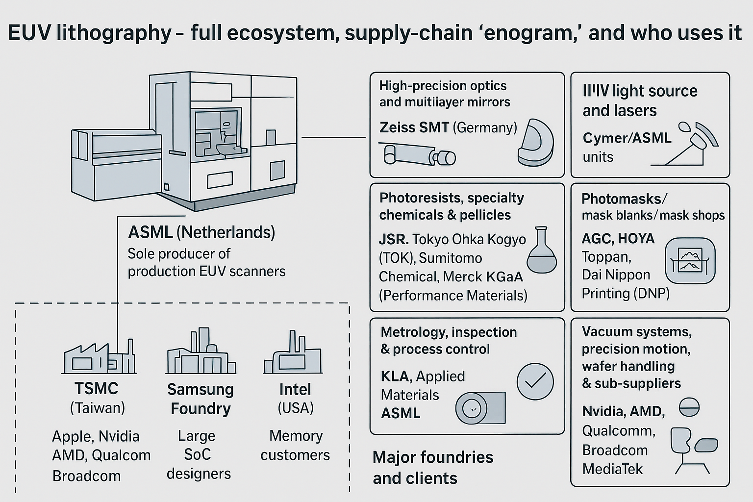
So where does the constraint actually sit? The EUV equipment supply chain is not a single bottleneck. It is a series of them, arranged in a daisy chain that stretches from a tin droplet generator in San Diego to a helium liquefaction plant in Qatar. Break any link and the whole line slows. Right now, three links are drawing particular scrutiny: the optical subsystem supply for High-NA tools, the helium supply for laser excitation and wafer-stage cooling, and the photoresist chemistry required to pattern at sub-13.5 nm half-pitch.
The optical subsystem is the most structurally constrained. Each High-NA EXE:5000 system requires an anamorphic projection optic with a numerical aperture of 0.55, fabricated by Carl Zeiss SMT in Oberkochen, Germany. Zeiss produces these mirror assemblies at a cadence that, according to two process integration engineers familiar with the matter, has not materially accelerated since 2024. The mirrors require months of ion-beam figuring and angstrom-level metrology per surface. ASML has not publicly disclosed its High-NA optic throughput, but the pace of EXE:5000 installations, roughly six to eight systems in 2025, with a target of 12 to 15 in 2026, implies a Zeiss output ceiling that is the gating factor for the entire High-NA ramp.
Then there is helium. The gas is non-negotiable for EUV lithography: it is used as a buffer in the laser-produced plasma source, as a coolant for the wafer stage, and as a purge gas in the optical path to prevent carbon deposition on the mirrors. In April, Forbes reported that disruptions at Qatar's Ras Laffan Industrial City, which supplies roughly 30 percent of the world's refined helium, had tightened the market to a degree not seen since the 2013-2014 shortage. Francis Sideco of TIRIAS Research wrote that "helium gas powering the world's most advanced semiconductor processes is suddenly in short supply, threatening to slow down production of the chips driving the AI boom." The DigiTimes helium supply analysis from late March pegged spot prices up 160 percent year-on-year, with allocation cuts hitting Asian fabs hardest.
The global helium market is currently facing an unprecedented supply shock, driven by geopolitical instability in the Middle East., DigiTimes supply chain analysis, March 2026
The photoresist picture is less acute but structurally similar. EUV photoresists are a formulation problem that sits at the intersection of photon absorption, acid diffusion, and etch resistance, three properties that trade against each other. The market, currently valued at roughly $1.32 billion according to Growth Market Reports research cited by Silicon Semiconductor, is projected to reach $10.8 billion by 2033. The dominant suppliers, JSR, Tokyo Ohka Kogyo, Shin-Etsu Chemical, and DuPont, are all expanding capacity, but qualification cycles for new resist formulations at 3 nm and below can take 18 months. TSMC's N2 process, which entered risk production in late 2025, uses EUV for more than 20 layers; each layer requires a specific resist tuned for its particular pitch and topography.
Against this backdrop of supply-side strain, TSMC dropped a decision in late April that reset the conversation about High-NA EUV adoption timelines. The company disclosed it would delay deploying ASML's High-NA tools for volume production until 2029, opting instead to extend its existing low-NA EUV fleet with advanced packaging and multi-patterning techniques. Bloomberg's Ian King and Debby Wu reported the decision with characteristic understatement: "TSMC Says ASML's Latest Chipmaking Gear Is Too Pricey to Use." Reuters noted that TSMC simultaneously unveiled its A13 and N2U process technologies, both built on existing EUV tools, alongside a new chip-packaging approach for AI accelerators.
The price tag in question is widely understood to be approximately €350 million per High-NA system, roughly double the cost of a top-spec low-NA NXE:3800E. For a fab running 30,000 wafer starts per month at the leading edge, the amortization math on a €350 million tool pencils out only if the process can eliminate enough multi-patterning steps to offset the higher capital cost. TSMC's engineers evidently concluded that for the N2 node and its derivatives, A13, scheduled for 2027, and N2U, scheduled for 2028, the equation does not close. Intel, by contrast, has already installed High-NA systems at its Oregon and Arizona sites for the 18A node, betting that single-exposure EUV at 0.55 NA will provide a defect-density advantage that justifies the premium. Samsung has taken a middle path, accepting one High-NA system for R&D at its Hwaseong campus while keeping its Pyeongtaek production lines on low-NA tools through at least 2028.
What this means for ASML is nuanced. The company is not losing revenue, TSMC's capex, forecast to hit $52 billion to $56 billion in 2026 according to DigiTimes reporting by Monica Chen, is still overwhelmingly directed at low-NA EUV and deep-ultraviolet immersion tools. ASML shares dipped 3.3 percent on the TSMC news and then largely recovered within the week, as analysts absorbed the fact that the delay does not reduce near-term EUV unit demand; it merely reshapes the product mix.
This product-mix question is where the EUV equipment supply chain intersects with geopolitics. The United States' MATCH Act, introduced in early 2026, explicitly targets third-party resale of advanced lithography equipment to Chinese entities. ASML's China revenue, which accounted for roughly 29 percent of total sales in 2024, has already been constrained by Dutch export controls aligned with the Wassenaar Arrangement. The new legislation would further restrict the flow of used and refurbished EUV systems, a secondary market that Chinese fabs had been exploiting to build out their domestic 7 nm capacity. ASML management has publicly stated it can "accommodate" the export controls, but the revenue rebalancing is real: every system that cannot be sold into China must find a buyer elsewhere, and the elsewhere buyers, TSMC, Samsung, SK Hynix, Intel, Micron, are already at the front of the queue.
Meanwhile, the Chinese domestic EUV effort, long dismissed as a science project, is beginning to register on equipment-vendor radars. Simply Wall St. reported in March that Chinese semiconductor firms and policymakers are "ramping up efforts to build domestic EUV lithography capability," focusing on a laser-produced plasma source developed at the Shanghai Institute of Optics and Fine Mechanics. No serious observer expects a production-ready Chinese EUV tool before 2030 at the earliest. But the procurement of subsystem components, precision stages, metrology modules, vacuum chambers, is being tracked by export-control enforcement agencies as a leading indicator. The component supply chain for EUV is so specialized that any surge in orders for, say, carbon-contamination-resistant mirror coatings from a previously unknown entity in Shenzhen is immediately legible to the small number of firms that manufacture those coatings.
The equipment supply chain beyond the headline ASML-Zeiss duopoly deserves more attention than it typically receives. Each EUV scanner contains roughly 100,000 components sourced from approximately 5,000 suppliers, a number that ASML's own investor presentations cite. Among the less visible but structurally critical suppliers: VDL ETG, which builds the wafer-stage and reticle-stage modules in Eindhoven; Berliner Glas (now owned by ASML), which fabricates the electrostatic chucks and optical modules; and Cymer, the San Diego-based subsidiary that produces the CO2 laser systems driving the tin-plasma light source. Cymer's lasers operate at 40 kilowatts of average power in the latest NXE:3800E configuration, up from 25 kW in the NXE:3400C. Each step increase in source power requires re-engineering the tin delivery system, the collector mirror cooling, and the debris mitigation scheme, a cascade of interlocking redesigns that ripples through the entire supplier base.
What the Low-NA to High-NA Transition Actually Changes
The High-NA EUV platform shifts the numerical aperture from 0.33 to 0.55, which reduces the minimum printable half-pitch from roughly 13 nm to 8 nm in a single exposure. The trade-off is the anamorphic lens design: the projection optic demagnifies the reticle image by 8x in one axis and 4x in the orthogonal axis, producing a half-field exposure of 26 mm by 16.5 mm instead of the full 26 mm by 33 mm of low-NA systems. For chip designers, this means reticle stitching is required for any die larger than 26 mm by 16.5 mm, which includes essentially every AI accelerator in production today. The stitching penalty, in terms of overlay error and throughput, is the central technical objection that TSMC's process integration team has raised, privately and now publicly, against near-term High-NA adoption for logic.
Memory makers face a different calculus. DRAM cell arrays are highly repetitive, which makes them amenable to half-field exposures without stitching. SK Hynix's $8 billion EUV order is directed primarily at 1c-nm DRAM production, where EUV is used for critical layers in the peripheral circuit region and for bit-line patterning. Samsung is applying EUV to its 1b-nm DRAM node with a similar pattern. For memory, the economic argument for High-NA is simpler: fewer multi-patterning steps per layer directly reduce process cycle time, and in a commodity market where cost-per-bit is the only metric that matters, cycle-time reduction translates cleanly to margin. That is why SK Hynix is outspending every other memory maker on EUV procurement in 2026, a fact that supplies its own quiet drama in a supply-constrained market.
Applied Materials and Tokyo Electron, the two largest equipment vendors after ASML, are positioning themselves as beneficiaries of the EUV ecosystem expansion rather than direct competitors. Neither company competes in lithography. Instead, they sell the deposition, etch, and metrology tools that surround the EUV scanner in a modern process flow. A single EUV layer in an N2 logic flow might require three to four deposition steps, two etch steps, and five metrology steps, all of which generate revenue for AMAT and TEL. Zacks Equity Research noted in a 2025 comparison that both AMAT and ASML "stand out as pivotal players in the semiconductor equipment landscape," but their growth trajectories are tied to different phases of the fab buildout cycle. AMAT benefits earlier, during the initial deposition-and-etch equipment installation; ASML benefits later, when the lithography layer count increases with process maturity. In the current cycle, both phases are running simultaneously, which is why WFE, wafer fab equipment, spending is forecast by SEMI to surpass $140 billion in 2026.
The EUV photoresist supply chain, often treated as an afterthought in equipment discussions, is where the next crisis is incubating. Current chemically amplified resists (CARs) are approaching their resolution limit at around 12 nm half-pitch, which is adequate for low-NA EUV but insufficient for High-NA single-exposure patterning of the 8 nm features that the EXE:5000 is theoretically capable of resolving. Metal-oxide resists, formulations based on hafnium, zirconium, or tin oxide nanoclusters, offer higher resolution and better etch resistance, but their sensitivity is roughly one-third that of CARs, meaning they require three times the dose to pattern. In a system where source power is the primary throughput constraint, a threefold dose penalty is commercially unviable. The resist suppliers, JSR, DuPont, and the Japanese chemical conglomerates, are therefore racing to develop high-sensitivity metal-oxide resists that can match CAR throughput at 8 nm half-pitch.
It is worth pausing to consider what "the physics says no" means in practical terms. EUV photons at 13.5 nm have an energy of approximately 92 electron-volts. When such a photon is absorbed by a resist molecule, it ejects a photoelectron that cascades through the material, generating secondary electrons that drive the acid-generation chemistry. The mean free path of these secondary electrons is on the order of 2 to 4 nm, which sets a fundamental blur on the latent image. At 8 nm half-pitch, the blur is a substantial fraction of the feature size. Overcoming it requires either shorter electron mean free paths, which means denser resist films, or clever post-exposure processing to sharpen the chemical gradient. Both approaches are being pursued, but neither is in volume production.
What to Watch Between Now and SPIE 2027
The next milestone for the EUV supply chain is not an earnings report. It is the delivery cadence of High-NA optics from Zeiss in the second half of 2026. If Zeiss ships eight or more 0.55 NA projection systems before year-end, ASML can credibly claim that the High-NA ramp is on track, TSMC's delayed adoption notwithstanding. If Zeiss ships five or fewer, the entire 2027 High-NA revenue assumption embedded in ASML's guidance, roughly €7 billion to €9 billion from High-NA alone, comes into question.
The secondary milestone is helium. The Ras Laffan disruption is not a one-quarter event. Helium liquefaction infrastructure has lead times measured in years; the Qatar facility that went partially offline in early 2026 will not return to full capacity before mid-2027, and the strategic helium reserve in the United States was sold down in the early 2020s. Fabs are responding with helium recycling systems that can recover 80 to 90 percent of the gas from EUV tool exhaust, but retrofitting a running fab with recycling plumbing is a months-long exercise that reduces tool availability. The first chipmaker to publicly cite helium as a production constraint, and one will, will shift the narrative from "supply chain is tight" to "supply chain is broken."
A third checkpoint, less visible but in some ways more consequential, is the qualification of metal-oxide resist at a major logic manufacturer. Intel has been the most aggressive in evaluating non-CAR resists for its 18A node, and a production qualification announcement, likely at the SPIE Advanced Lithography + Patterning conference in February 2027, would signal that the resist physics barrier is surmountable. If no such announcement materializes, the High-NA roadmap begins to look like a tool platform in search of a chemically compatible process window, which is exactly the scenario that TSMC's delay decision implicitly anticipates.
Christophe Fouquet, at the AGM in April, was asked directly about the TSMC delay. His reply, as paraphrased by one attendee, was characteristically dry: the industry has always adopted new lithography in stages, and demand for EUV of any kind remains well above supply. The statement is factually correct and strategically incomplete. The EUV supply chain is not a single question of "do we have enough tools?" It is a set of interdependent constraints, optical, chemical, thermal, and political, that tighten in lockstep as the AI capex cycle accelerates. The number to watch is not €36 billion. It is the 40-kilowatt laser burn-in time at Cymer, the mirror-shipment cadence from Oberkochen, the helium spot price in Seoul, and the electron mean free path in a tin-oxide nanocluster film. Those numbers will tell you, months before any earnings release, whether the industry can build what it has promised.
Read next
