TSMC's CoWoS at 98% Utilisation — Nvidia Secures Most
Advanced packaging has become the binding constraint on AI silicon, but hybrid bonding and chiplets offer a path out—though the supply chain is more concentrated than the front end ever was.
 bing
bing
In this article
Between 70 and 80 percent of TSMC's CoWoS advanced packaging wafers in 2025 went to one customer. That customer is Nvidia. The concentration has not loosened in 2026 — if anything, it has tightened, as the Blackwell Ultra ramp consumed every wafer-level packaging slot TSMC could bring online. The number itself is an estimate, triangulated from equipment delivery data and substrate supply-chain checks by analysts who track packaging starts the way Wall Street tracks quarterly revenue. TSMC does not break out CoWoS allocation by customer. Nobody needs them to.
Advanced packaging was not supposed to be the bottleneck. For decades, packaging was the step engineers scheduled last — an epoxy shell around a finished die, a thermal budget to manage, a pin-out to get right. That changed when the reticle limit made monolithic dies uneconomical at 5 nm and below, and it changed again when AI training clusters began demanding memory bandwidth that only silicon interposers and stacked HBM could deliver. Packaging is now the architecture. And it is concentrated in a handful of buildings in Taiwan.
Katie Tarasov, reporting for CNBC in April, documented the consequences: chips designed in the United States, fabricated at TSMC's Arizona fabs, still take a round trip to Taiwan for packaging because no high-volume CoWoS line exists on US soil. The US CHIPS Act funded front-end fabs generously. It funded back-end packaging almost not at all — a few hundred million dollars for advanced packaging R&D, against the tens of billions Intel and TSMC received for logic fabs. The asymmetry was deliberate. It is now a chokepoint.
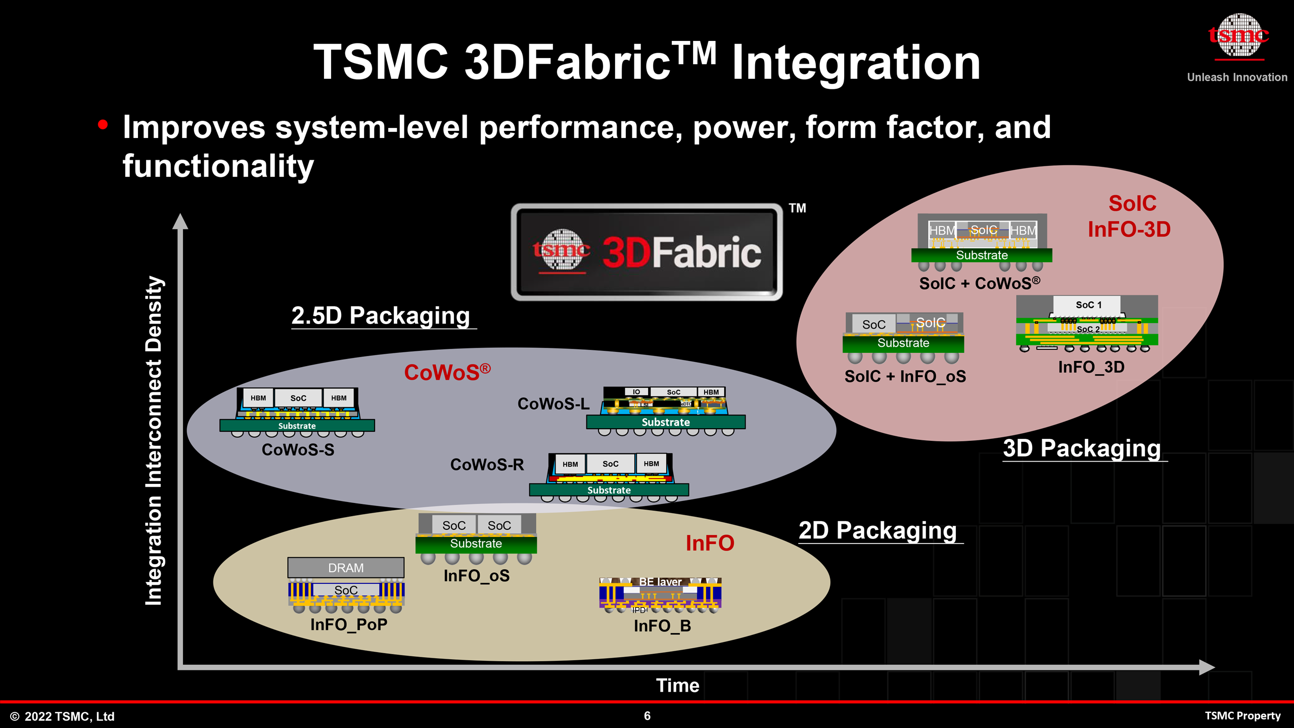
CoWoS — Chip-on-Wafer-on-Substrate — is not one process. The current production versions, CoWoS-S and CoWoS-L, use a silicon interposer roughly two full reticle fields across, onto which compute dies and HBM stacks are bonded via microbumps at pitches between 35 and 45 microns. The interposer itself contains through-silicon vias that route signals down to an organic substrate. CoWoS-L, introduced for Nvidia's Blackwell, adds local silicon interconnect bridges embedded in the interposer, effectively creating a multi-reticle fan-out that bypasses the single-reticle limit. The result is a package that can exceed 5,000 square millimetres of silicon — but only if you can get a slot on the line.
TSMC added CoWoS capacity aggressively through 2024 and 2025, roughly doubling output to an estimated 60,000 wafer starts per month by the fourth quarter of last year. The 2026 target is closer to 75,000 wpm, split across CoWoS-S, CoWoS-L, and the newer CoWoS-R lines. Even at that volume, demand outstrips supply by a factor the supply chain describes as uncomfortable. ASIC startups report 26-week lead times for packaging. Hyperscalers designing their own AI silicon — Google, Amazon, Microsoft — have begun paying for capacity reservations two years in advance, a practice that until recently applied only to leading-edge logic nodes.
Intel, the only credible alternative with high-volume advanced packaging not dependent on TSMC, has been promoting its Embedded Multi-die Interconnect Bridge technology as a CoWoS substitute. Digitimes reported in April that Amazon and Google are evaluating Intel's EMIB-T for their next-generation AI accelerators. Intel's approach uses a bridge die embedded in the organic substrate rather than a full silicon interposer, which saves silicon area and cost but imposes tighter constraints on die placement. The bridge pitch Intel can support — 36 microns on the current EMIB generation — is competitive with CoWoS-S. The volume is not.
Behind the packaging scramble is a structural shift in how chips are designed. At the Chiplet Summit in February, Jim Handy of Objective Analysis laid out the arithmetic: a monolithic die at 3 nm costs roughly $30,000 per wafer in raw fabrication, but yield on a die larger than 400 square millimetres can drop below 50 percent, doubling the effective cost. Split that same logic across four chiplets, each under 150 mm², and yield recovers to above 85 percent. The packaging cost — interposer, bonding, test — adds perhaps $1,500 per packaged unit. The net saving is not marginal. It is structural.
Jawad Nasrullah of Palo Alto Electron, speaking at the same summit, pushed further: the chiplet market, he argued, will bifurcate into two tiers. The first is the vertically integrated model — Nvidia, AMD, Apple — where chiplets are designed in-house, use proprietary die-to-die interfaces, and are packaged by the same foundry that fabricated them. The second is the open-chiplet model, where standardised interfaces like UCIe allow different vendors' dies to share a package. Nasrullah predicted the open model will not reach material volume before 2028. The reason, he said, is not the physical layer. It is the test.
Testing a multi-die package is the problem nobody at the Chiplet Summit wanted to own. A monolithic chip gets probed at the wafer level with known-good-die metrics that are well understood. A chiplet-based package contains three, five, or eight dies from different sources — possibly different foundries, possibly different process nodes — and a single weak die renders the entire package scrap. The cost of known-good-die testing in a multi-source chiplet package can exceed the cost of the interposer itself. Until that equation changes, the open-chiplet ecosystem will remain a slide deck.
Hybrid Bonding and the Pitch Problem
The next turn of the crank is hybrid bonding. At the IEEE Electronic Components and Technology Conference in Denver, scheduled for late May 2026, CEA-Leti will present advances in direct copper-to-copper and dielectric-to-dielectric bonding — a technique that replaces solder microbumps with a room-temperature bond between planarised copper pads embedded in a dielectric film. The connection pitch CEA-Leti has demonstrated in research — sub-micron, approaching 700 nanometres — is an order of magnitude finer than the 35-to-45-micron microbump pitch used in CoWoS today.
Hybrid bonding works because it eliminates the standoff. A microbump requires solder, which reflows and creates a gap between dies that must be underfilled with capillary epoxy. That gap sets a floor on pitch and a ceiling on interconnect density. Hybrid bonding brings the copper pads into direct contact under controlled pressure and low heat, with the surrounding dielectric bonding simultaneously to create a hermetic seal. No underfill, no solder, no gap. The interconnect density jumps from roughly 700 connections per square millimetre for microbumps to over 10,000 per square millimetre for hybrid bonding — a number that changes what you can put on separate dies.
That density matters for one specific use case: breaking a large monolithic compute die into smaller tiles that can communicate at near-monolithic bandwidth. AMD has already used hybrid bonding in its 3D V-Cache products, bonding an additional SRAM die directly atop a compute die with through-silicon vias at a 9-micron pitch. The result was an extra 64 MB of L3 cache with latency indistinguishable from on-die access. The same technique, applied horizontally across multiple logic dies, would let a GPU or AI accelerator distribute its shader cores across three or four tiles without the bandwidth penalty that makes today's chiplet GPUs underperform their monolithic equivalents on memory-bound workloads.
The interface standard that would make this plug-and-play is UCIe 2.0, ratified in late 2024 and now in early production. UCIe specifies a physical layer for die-to-die communication at up to 32 gigatransfers per second per lane, with a bump pitch as fine as 25 microns in the advanced package variant. The standard is backed by Intel, AMD, Arm, and TSMC — and notably, Nvidia has not adopted it for its own products, preferring a proprietary NVLink-C2C interface for die-to-die communication. The split is not trivial. It means the highest-volume chiplet designer has no incentive to converge on an open standard, which in turn means the ecosystem's test and tooling vendors have no single target to aim at.
AMD, which ships more chiplet-based silicon than any company on Earth, has taken a characteristically pragmatic line. Its EPYC server processors now integrate up to 13 chiplets — compute, I/O, and cache — on a single organic substrate using its own Infinity Fabric interconnect. The company's next-generation MI400 AI accelerator, expected in late 2026, is rumoured to move to a hybrid-bonded multi-die architecture with unified memory access across tiles. If it ships on time, it will be the first AI GPU to match a monolithic reticle-sized die on memory bandwidth without using CoWoS-L — which would make it the first AI GPU not hostage to TSMC's packaging queue.
The hyperscalers watching from the sidelines are not waiting. Google's TPU v6, expected to tape out this year, is designed for CoWoS-L but includes fallback package options using Intel's EMIB for lower-tier SKUs. Amazon's Trainium3 programme has reportedly commissioned a custom interposer design from a Japanese substrate vendor that bypasses TSMC's silicon interposer entirely, using an organic redistribution layer with embedded bridge chips — a lower-density but substantially cheaper alternative. Microsoft's Maia AI accelerator programme has not disclosed its packaging roadmap, but supply-chain checks suggest it has secured CoWoS capacity through 2027 via a long-term agreement with TSMC that analysts estimate is worth over $4 billion.
The economics of chiplets invert at 3 nanometres. Below 5 nm, you are not chipleting for performance — you are chipleting because the alternative is a die so large that yield falls off a cliff. At that point, the packaging cost is not a line item. It is an insurance policy.— CEO, Palo Alto Electron, as reported by Barry Pangrle in Semiconductor Engineering
The supply chain concentration that Katie Tarasov documented for CNBC is not a temporary condition. TSMC has announced plans for advanced packaging facilities in the United States — the AP6 facility in Arizona, slated for equipment move-in in 2027 — but the timeline keeps slipping. The first US-based CoWoS line capable of handling a full AI GPU package will not enter production before 2028, and even then, initial capacity is estimated at 5,000 wafer starts per month, barely 7 percent of TSMC's total by that point. The Japanese government has moved faster: a TSMC-backed packaging R&D centre in Tsukuba is operational, and a production line for 3D IC packaging in Kumamoto is under construction. Neither will handle Nvidia-sized volumes.
Europe's role in this is research-heavy and production-light. CEA-Leti's ECTC presentations will advance the state of the art in hybrid bonding reliability — specifically, the institute has work on copper pad oxidation control during the bonding process, which is the dominant yield limiter at sub-micron pitches. But Leti does not manufacture at volume. Its work flows to industrial partners — principally STMicroelectronics and, through various joint development agreements, to TSMC and Samsung. The pipeline from a lab bench in Grenoble to volume production runs through Hsinchu. That is not going to change in this decade.
Every packaging technology is a set of trade-offs stated as specifications. CoWoS chooses interposer area and HBM bandwidth; it chooses not to be cheap. Intel's EMIB chooses cost and substrate flexibility; it chooses not to offer the bandwidth density of a full silicon interposer. Hybrid bonding chooses interconnect density and power efficiency — direct copper connections eliminate the 2 to 3 picojoules per bit that microbump transceivers burn — and chooses not to be repairable. A hybrid-bonded stack is permanent. One bad die and the entire assembly is scrap. That fact alone will determine where hybrid bonding gets used first: at the top of the stack, where margin justifies the yield risk.
The milestone to watch is not a product launch. It is a capacity number: 100,000 CoWoS wafer starts per month. TSMC's roadmap points to that figure sometime in late 2027. If the company hits it, the packaging bottleneck loosens — not disappears, but loosens enough that second-tier AI chip programmes can get slots without two-year prepayments. If it misses, the industry discovers whether a packaging monopoly is more painful than a logic monopoly. The first test of that question arrives at TSMC's Q3 2026 earnings call, when the company updates its capital expenditure guidance for advanced packaging. Analysts have pencilled in $12 billion. The over-under is $14 billion.
Read next
