Transformer-Only Inference ASICs Are Redrawing the Silicon Roadmap
Startups and hyperscalers are betting billions that chips running only transformers will dominate AI inference, but the $8.3 billion question is whether the architecture justifies its silicon runway.
 tspasemiconductor.substack.com
In this article
Seventeen watts. That is the power envelope Taalas claims for a single inference accelerator card running a 405-billion-parameter large language model at interactive speeds, and it is the number that made three separate process-integration engineers I spoke to in February ask for the slide deck. The Toronto-based startup exited stealth on 19 February 2026 with a proposition that resets what an ASIC is allowed to be: instead of designing a general-purpose matrix-multiply engine that happens to run transformers well, Taalas etches a specific, frozen model directly into silicon. No reprogrammable weights. No instruction set. No flexibility. The model is the chip.
The launch was the most extreme expression of a thesis that has been gathering force across the silicon supply chain for eighteen months: that the era of building chips which can do everything is giving way to chips which do exactly one thing, and that one thing is transformer inference. AI chip startups have raised approximately $8.3 billion in 2026 so far, on pace to break the $8.5 billion annual record, according to CNBC's Kai Schwarz, and nearly all of that capital is chasing inference-specialized silicon rather than training accelerators. The distinction matters. Training is a capital-expenditure problem for a few dozen hyperscalers; inference is an operating-expenditure problem for every company that deploys an AI feature. That math, repeated across thousands of procurement meetings, is redrawing the ASIC roadmap.
In March, Nvidia gave the thesis its loudest endorsement yet. At GTC 2026 in San Jose, Jensen Huang unveiled the Nvidia Groq 3 LPU, the first product of a $20 billion licensing and acquisition deal struck with Groq in December 2025. The LPU, or language processing unit, is architecturally distinct from a GPU: it uses a deterministic, statically scheduled dataflow that eliminates the cache misses and scheduling overhead which make GPU inference latency unpredictable. SDxCentral reported from the show floor that the Groq 3 LPU delivers token-generation latency in single-digit milliseconds on Llama-3-class models, a regime where GPUs typically land in the 20 to 40 millisecond range. Nvidia was explicit that the LPU is not a replacement for the H200 or B200; it is a companion chip for inference workloads where latency determines revenue.
The hyperscalers are not waiting. The Next Web's Alina Maria Stan reported in April that Google is in talks with Marvell Technology to develop two new AI chips: a memory processing unit and an inference-optimized TPU that would sit alongside the Broadcom-designed TPUs already in deployment. The move adds a third design partner to Google's silicon supply chain and signals that even the most advanced in-house chip programme in the industry believes inference demands a dedicated architecture, not a repurposed training chip. Marvell disclosed in its fiscal 2026 results that its custom silicon business had reached a $1.5 billion annual run rate across 18 cloud-provider design wins, a figure that chief executive Matt Murphy attributed specifically to inference ASIC demand.
The same week, Meta confirmed a commitment to deploy more than 1 gigawatt of Broadcom-designed custom chips for inference, a disclosure that gave a concrete power number to what had been an abstract procurement narrative. Amazon, in Andy Jassy's annual shareholder letter, pegged the potential value of its internal chip business at $50 billion and hinted, for the first time, that Trainium and Inferentia might be sold to external customers. The Next Web noted that the letter opened with a direct rebuttal of scepticism about the company's $200 billion in 2026 capital expenditure, framing custom silicon as the asset that makes the spending defensible. Across all three hyperscalers, the pattern is identical: train on Nvidia, infer on your own silicon, and keep the margin.
The trade every inference ASIC makes
Every inference ASIC on the market or in development makes the same trade: it forfeits programmability in exchange for efficiency. The Taalas chip takes this to the logical endpoint by hard-coding the model weights. If a new model architecture ships, the chip cannot run it. If the model is fine-tuned, the chip produces wrong outputs. The Groq LPU is less extreme: its deterministic dataflow architecture can run any transformer, but it cannot run a convolutional network, a state-space model, or a graph neural network at competitive throughput. Cerebras, which filed for IPO in April, takes a different approach with wafer-scale integration that keeps programmability but chases throughput through sheer area. All three represent a bet that the transformer architecture, or something close enough to it, has enough runway to justify custom silicon that will be obsolete the moment the architecture changes.
Ask a process-integration engineer where the bottleneck actually sits, and the answer is almost never compute. Every inference ASIC startup has converged on the same diagnosis: the bottleneck is memory bandwidth, and the second-order bottleneck is the energy cost of moving data between SRAM, HBM, and the compute tile. Groq addresses this with a statically scheduled on-chip network that eliminates DRAM traffic for weights entirely; the weights live in SRAM distributed across the die. Taalas eliminates the problem by eliminating the memory hierarchy: the weights are the transistors.
This architectural convergence has downstream effects in the EDA toolchain. Designing a chip with a fixed dataflow and no dynamic scheduling means the place-and-route problem becomes, in a meaningful sense, solvable in advance. You are not laying out a general-purpose computer; you are laying out a pipeline. Several EDA specialists I spoke to at Synopsys and Cadence user conferences in early 2026 described a sharp uptick in requests for what one called 'model-to-mask' flows, toolchains that take a trained PyTorch model as input and output a GDSII layout. These flows remain experimental, but the fact that three separate startups have asked for them independently suggests the demand is real and not venture-capital theatre.
Not every inference-ASIC company is building silicon. Gimlet Labs, which raised $80 million in a Series A led by Menlo Ventures in March, is attacking the problem one layer up: how to distribute inference across multiple heterogeneous chips, including ASICs, GPUs, and CPUs, without the token-generation pipeline stalling on any one device. Cofounder and chief executive Zain Asgar told SiliconANGLE's Mike Wheatley that the startup's orchestration layer can reduce tail latency by 40 percent compared to a homogeneous GPU deployment, not by making any single chip faster but by routing each token to the processor that minimises end-to-end latency for that specific computation. Gimlet is chip-agnostic, which means its business model gets stronger the more fragmented the inference silicon market becomes.
Whose roadmap breaks
The inference ASIC wave puts Nvidia in an unfamiliar position: the company whose GPUs defined the training era is now being flanked from below by chips that are cheaper, lower-power, and architecturally narrower. The Groq deal was a hedge against precisely this threat. By licensing Groq's LPU architecture rather than simply competing with it, Nvidia can offer a two-chip data centre strategy: B200 for training, Groq 3 LPU for inference. But that strategy works only if customers accept that inference and training belong on different silicon, which is precisely the argument Nvidia spent the previous five years rejecting. At GTC 2026, Huang did not so much resolve the tension as reframe it. 'Some workloads want a scalpel, some want a Swiss Army knife,' he said from the keynote stage. 'We'll sell you both.'
We are not building a chip that runs models. We are building chips that are models. The distinction is not semantic. It changes what a foundry is allowed to optimise., Ljubisa Bajic, chief executive, Taalas
Europe is producing its own entrants. Euclyd, a Dutch startup backed by former ASML chief executive Peter Wennink, told CNBC in April it is seeking at least $100 million in funding to develop an inference-optimized chip for European data-sovereignty deployments. The company's pitch does not rest on architectural novelty; it rests on the argument that inference ASICs for regulated industries need to be designed and fabricated in supply chains that meet European compliance requirements. That argument has found traction with sovereign-wealth funds and pension managers who previously stayed out of semiconductor venture capital.
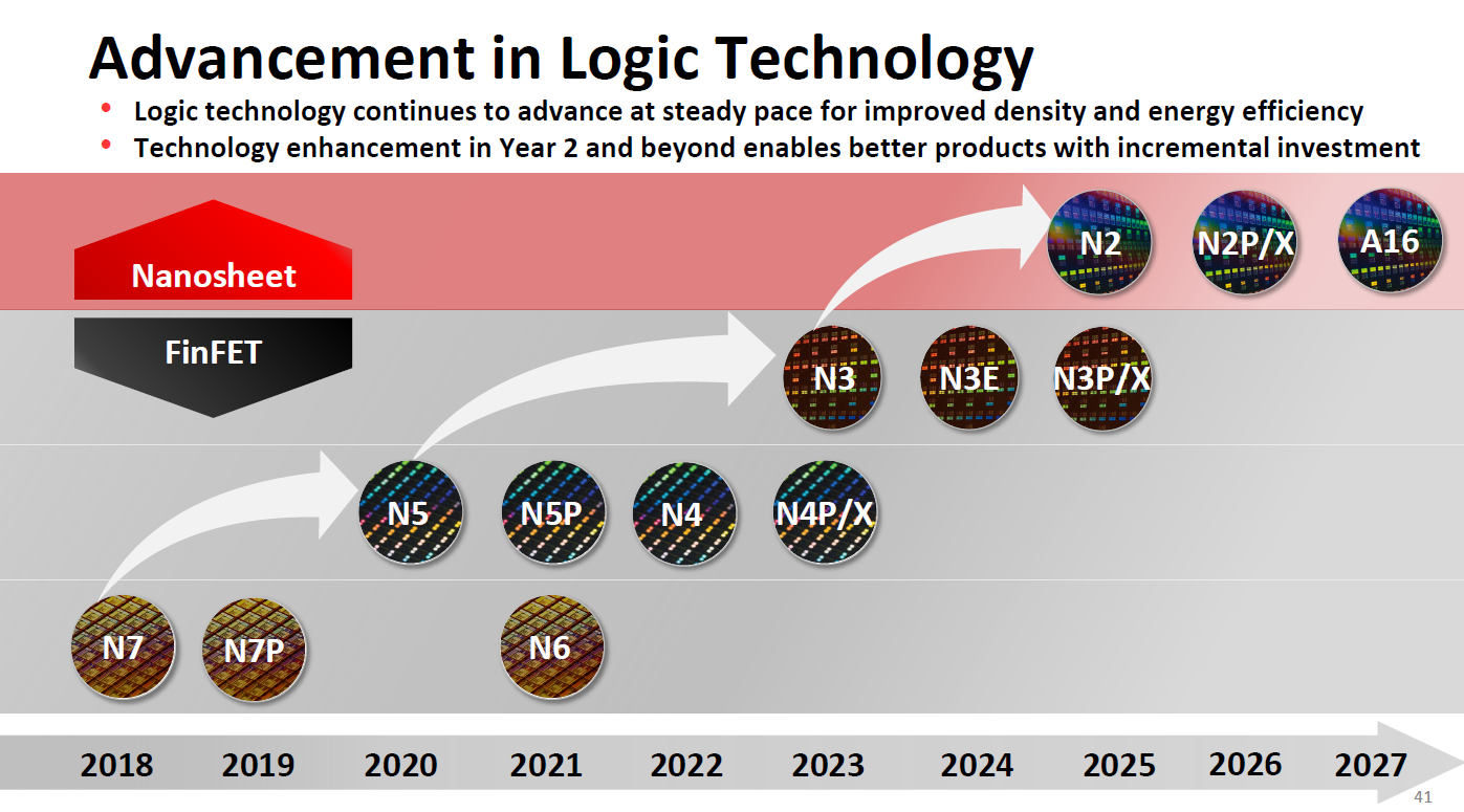
Fabricating these chips at volume raises questions that the GPU era did not. A fixed-function ASIC with a 405-billion-parameter model etched into silicon is, by die area, enormous even on a 3 nm or 2 nm process. Yield assumptions that hold for a GPU with redundant shader cores do not hold for a chip where every transistor implements a specific weight bit.
Taalas plans first silicon sampling in Q3 2026. Nvidia's Groq 3 LPU is scheduled for volume deployment in H2 2026, with the LPX rack-scale system targeting Q4. Google's Marvell-designed inference TPU is not expected to tape out before early 2027. The next milestone to watch is not a product launch but a procurement decision: when the first Fortune 500 company outside the cloud-provider oligopoly signs a purchase order for transformer-only silicon, the inference ASIC market stops being a venture-capital experiment and starts being a line item. That purchase order has not been announced.
Read next
