 Silicon · Inference ASICs
OpenAI's Jalapeño, Cerebras's wafer-scale benchmarks, and a 44.6% ASIC shipment surge confirm that transformer-only inference chips are no longer experimental, they are the industry's new default.
Jun 27, 2026
·
9 min
 Hardware · Advanced Packaging
As TSMC's CoWoS capacity struggles to meet AI silicon demand, MediaTek turns to Intel's embedded multi-die interconnect bridge technology for its AI ASIC production, signaling a split in advanced packaging orders that could reshape the foundry landscape.
Jun 17, 2026
·
9 min
Hardware · Chip Equipment
The EUV lithography supply chain, already strained by AI chip demand, now deals with helium shortages from Middle East instability, creeping Chinese equipment advances despite sanctions, and customer pushback on High-NA pricing.
Jun 7, 2026
·
9 min
 Hardware · Custom Silicon
Google forking its TPU into separate training and inference dies at 2nm signals that the AI chip market is splitting, and for inference-only ASICs the crucial design question is no longer what a chip can do but what it can leave out.
Jun 2, 2026
·
8 min
 Hardware · Silicon
Google, Meta, Amazon, and a wave of startups are designing silicon that runs transformers and nothing else. The general-purpose AI accelerator is being retired in real time.
May 28, 2026
·
10 min
Hardware · Silicon
As inference overtakes training, custom ASICs purpose-built for transformers from Google, Cerebras, and emerging startups are challenging the GPU monopoly and rewriting the semiconductor roadmap.
May 23, 2026
·
11 min
 Silicon · Supply Chain
As Nvidia reserves most of TSMC's CoWoS capacity, the industry scrambles for alternatives like hybrid bonding, reshaping chip design from substrate to interconnect pitch.
May 18, 2026
·
8 min
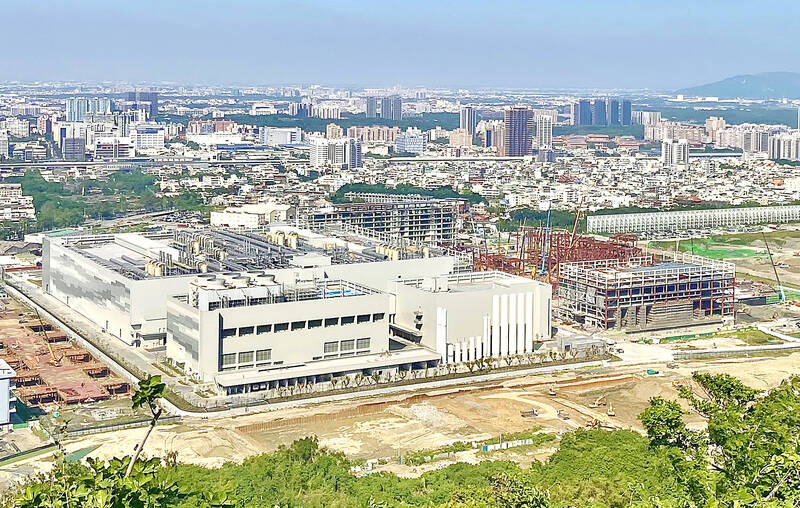
 Hardware · Geopolitics
TSMC's strategic fab placements across four jurisdictions reflect a shift where governments, not just markets, now dictate chip process node locations, and the 2028 production milestones will test whether this geopolitical experiment sustains the semiconductor supply chain.
May 14, 2026
·
7 min
 Hardware · Silicon Supply Chain
As AI demand overwhelms TSMC's advanced packaging monopoly, Intel, CEA-Leti, and emerging hybrid-bonding and chiplet technologies are racing to redefine how chips are stitched together.
May 13, 2026
·
11 min
 Hardware · Supply Chain
With CoWoS capacity booked through 2027 and hybrid bonding still emerging, chip designers are scrambling to rework roadmaps around the advanced packaging constraint that nobody saw coming.
May 12, 2026
·
9 min
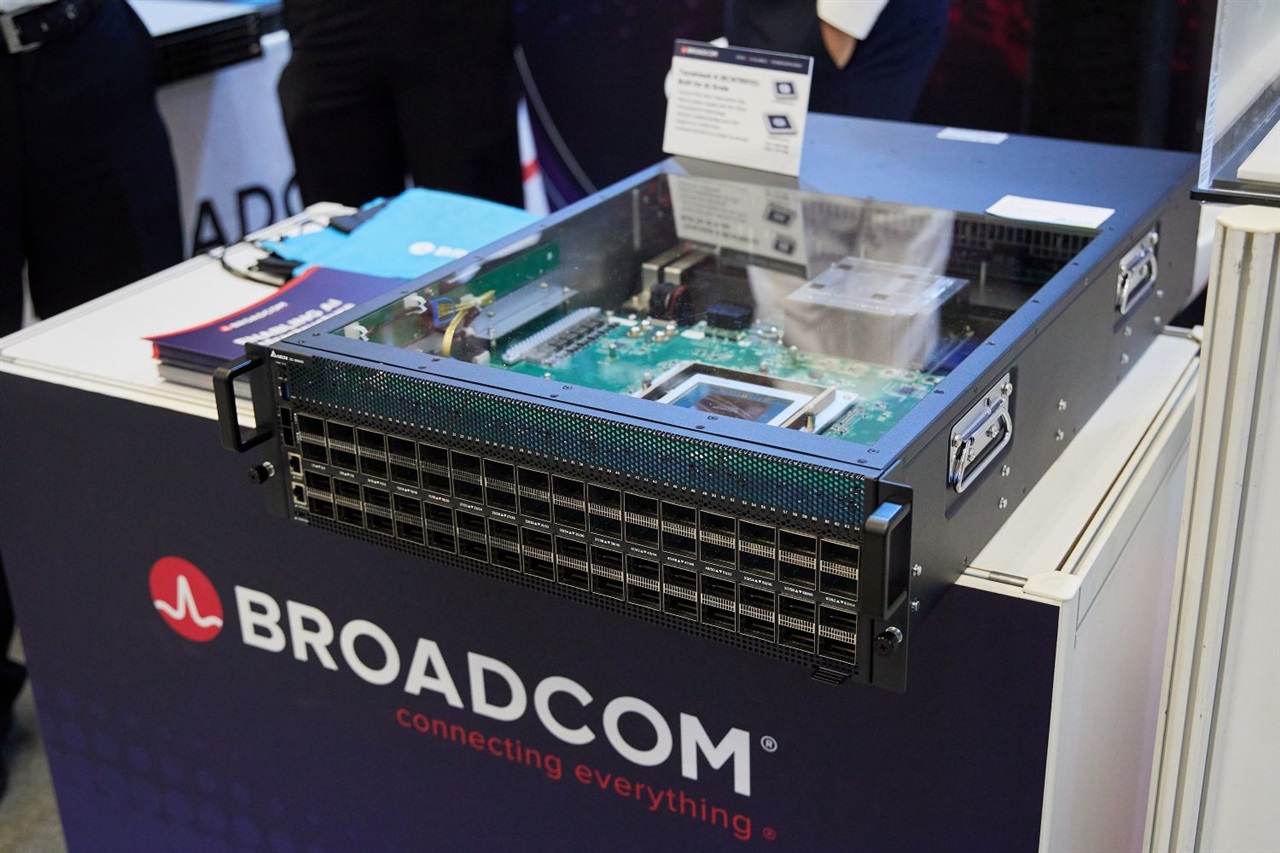
 Hardware · Inference ASICs
Transformer-specialized silicon sheds training circuitry to create a new class of inference ASICs optimized purely for token speed and power efficiency.
May 11, 2026
·
8 min
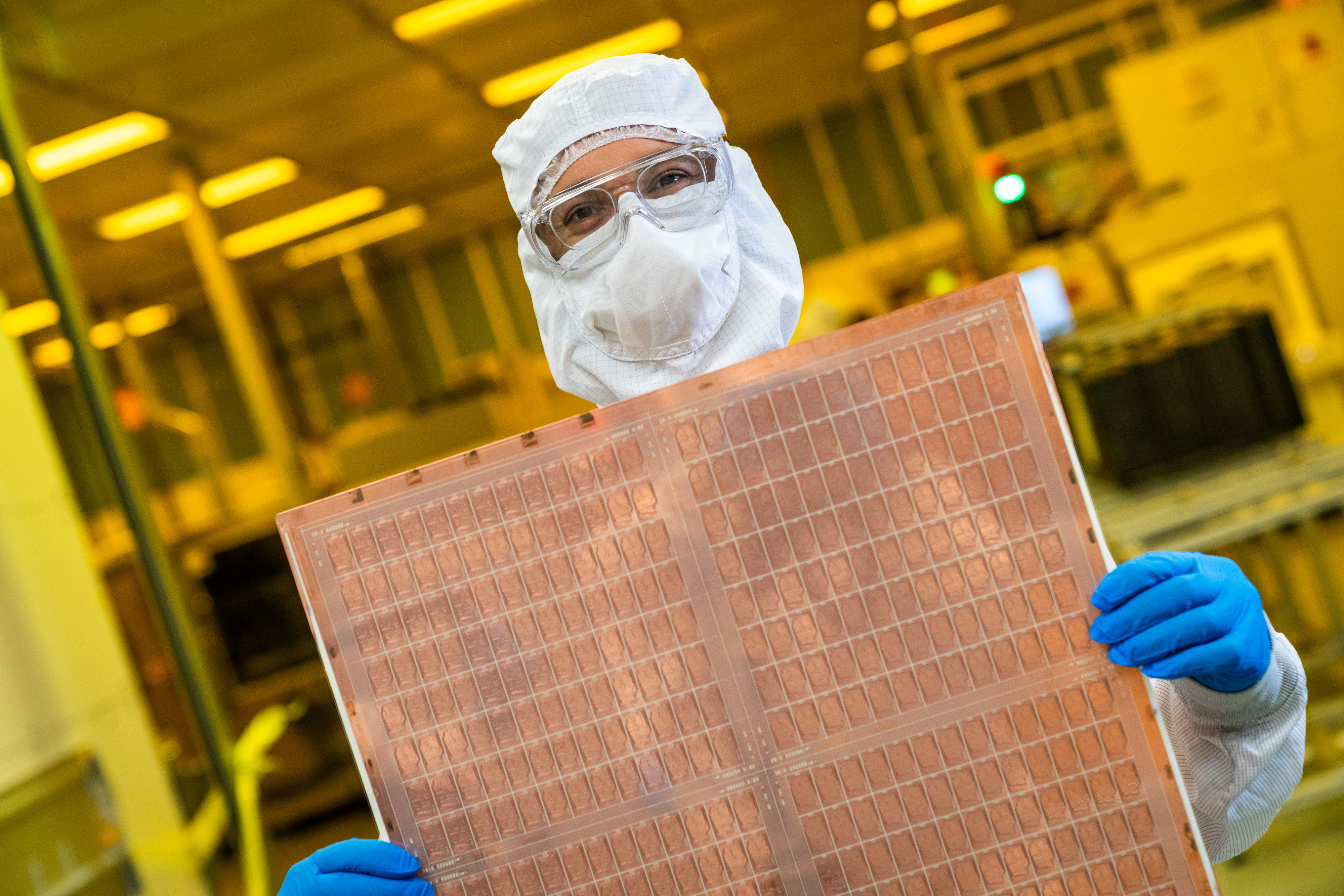
 Silicon · Foundry Process
TSMC's five 2nm fabs are selling every wafer through 2026 while Samsung and Intel struggle with yields, making defect density the defining factor in the advanced chip race.
May 11, 2026
·
9 min
 Hardware · Supply Chain
TSMC's upgrade of its second Japanese fab to 3-nanometer production is not a market move, but the latest proof that the geography of advanced silicon is now drawn by security planners, not supply-chain managers.
May 11, 2026
·
9 min
 Silicon · Supply Chain
ASML raised its 2026 revenue outlook to €40 billion, but the extreme ultraviolet lithography supply chain is maxed out, with optics, chemicals, and geopolitics straining under the load.
May 10, 2026
·
12 min
 Hardware · Silicon Design
Startups and hyperscalers are betting billions that chips running only transformers will dominate AI inference, but the $8.3 billion question is whether the architecture justifies its silicon runway.
May 9, 2026
·
7 min
 Packaging · Supply Chain
Advanced packaging has become the binding constraint on AI silicon, but hybrid bonding and chiplets offer a path out—though the supply chain is more concentrated than the front end ever was.
May 9, 2026
·
9 min
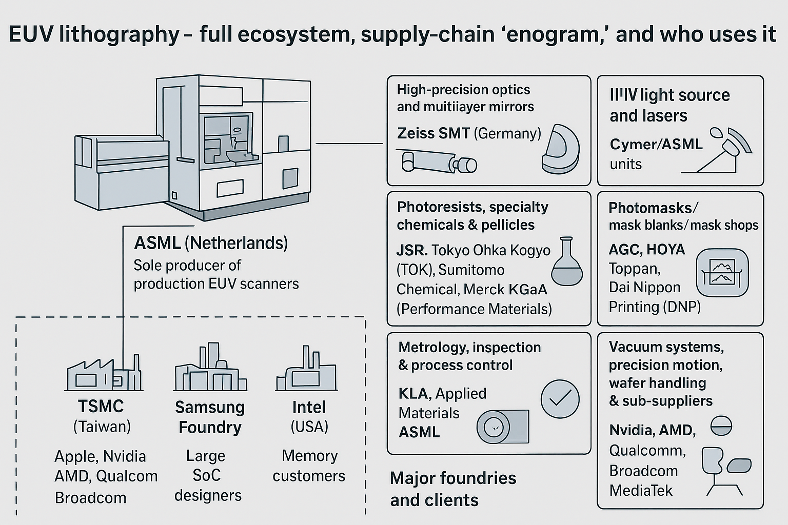
 Hardware · Silicon Supply Chain
While ASML's EXE:5200 High NA scanner ships and its light source targets 1,000 watts, the real bottleneck lies in a supply chain of 5,000 suppliers, where Zeiss mirrors and TRUMPF lasers each rely on a single factory on Earth.
May 9, 2026
·
9 min
 Hardware · Silicon
Five fabs entering volume production this year, 70% CAGR through 2028, $52-56B capex at the upper end of guidance. The 2nm capacity allocation is the supply chain story of the year.
May 8, 2026
·
2 min
 Hardware · Memory
Samsung Electronics passed $1T market cap on May 6. The earnings driver everyone is pointing at is the AI inference market. The actual driver is the HBM3e qualification cycle.
May 7, 2026
·
1 min
